
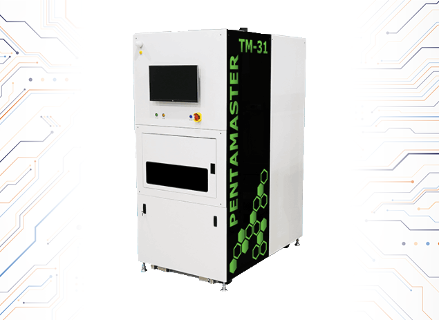
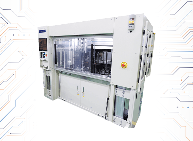
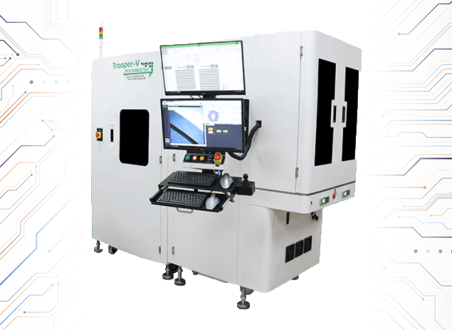
Trooper-V Wafer-Level AOI Handler
Trooper-V Wafer-Level AOI Handler Trooper-V is next level high speed AOI handler designed for wafer-level packages. In just 2 minutes, trooper v inspection system Is
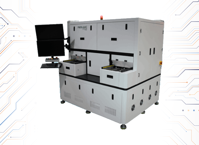
![]() 4JMSolutions is proud to offer advanced wafer Automatic Optical Inspection (AOI) systems from leading manufacturers. These systems play a crucial role in the semiconductor manufacturing process by ensuring accurate wafer mapping and defect detection. By investing in a reliable wafer AOI system, manufacturers can significantly enhance the efficiency, quality, and yield of their production processes.
4JMSolutions is proud to offer advanced wafer Automatic Optical Inspection (AOI) systems from leading manufacturers. These systems play a crucial role in the semiconductor manufacturing process by ensuring accurate wafer mapping and defect detection. By investing in a reliable wafer AOI system, manufacturers can significantly enhance the efficiency, quality, and yield of their production processes.
Wafer mapping is an essential aspect of semiconductor manufacturing, allowing for the precise identification of the location and orientation of each die on the wafer. This process ensures that only defect-free dies are selected for further processing, ultimately leading to higher overall product quality and reduced production costs.
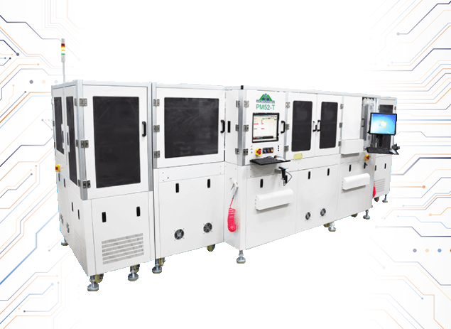
Our wafer AOI systems are designed with cutting-edge technology and built to deliver accurate, high-speed inspection capabilities. By utilizing advanced imaging techniques, these systems can rapidly and accurately detect defects on semiconductor wafers, enabling manufacturers to make informed decisions on wafer processing.
Some key benefits of wafer AOI systems include:
By incorporating a wafer AOI system from ![]() 4JMSolutions into your semiconductor manufacturing process, you can ensure that your operations remain competitive in this rapidly evolving industry. At
4JMSolutions into your semiconductor manufacturing process, you can ensure that your operations remain competitive in this rapidly evolving industry. At ![]() 4JMSolutions, we are committed to providing state-of-the-art equipment and exceptional customer support to help our clients achieve success in their manufacturing endeavors.
4JMSolutions, we are committed to providing state-of-the-art equipment and exceptional customer support to help our clients achieve success in their manufacturing endeavors.
Explore our range of wafer AOI systems and discover how ![]() 4JMSolutions can help your semiconductor manufacturing operations stay ahead of the competition. Contact us today for more information on our wafer AOI systems and learn how we can customize our offerings to meet your specific needs.
4JMSolutions can help your semiconductor manufacturing operations stay ahead of the competition. Contact us today for more information on our wafer AOI systems and learn how we can customize our offerings to meet your specific needs.

Trooper-V Wafer-Level AOI Handler Trooper-V is next level high speed AOI handler designed for wafer-level packages. In just 2 minutes, trooper v inspection system Is
![]() 4JMSolutions (Malta) Ltd. was founded in 2008 on a solid base of international servicing and more than 25 years of high end industrial experience. Based on the solid principal of providing solutions where the equipment offered is a biproduct of the solution.
4JMSolutions (Malta) Ltd. was founded in 2008 on a solid base of international servicing and more than 25 years of high end industrial experience. Based on the solid principal of providing solutions where the equipment offered is a biproduct of the solution.